

Ultrafast Lasers Transform Semiconductor Failure Analysis
Ultrashort-pulsed lasers are redefining physical failure analysis (PFA) in semiconductor manufacturing, offering rapid, precise, and contamination-free sample preparation for microstructure diagnostics. These lasers, operating in the picosecond to femtosecond range, enable site-specific removal of encapsulating materials or deep layers within complex packaging architectures, such as 2.5D and 3D integrated circuits. As heterogeneous integration becomes more prevalent, defects often reside far beneath the surface, demanding tools capable of reaching micrometer-scale targets without introducing artifacts.

Traditional mechanical methods and focused ion beam (FIB) systems have long been the mainstay for PFA sample preparation. Mechanical techniques require skilled personnel and are time-intensive, while FIB systems offer high precision but come with significant ownership costs and limited throughput. Ultrafast lasers present an alternative by delivering high fluences at optimal wavelengths, enabling multiphoton absorption to machine even transparent materials. The reduction of pulse length to the femtosecond scale minimizes thermal damage, confining heat-affected zones to less than a few hundred nanometers.
One of the key advantages of laser micromachining is the absence of elemental contamination or ion implantation effects. Ablation rates achieved with ultrafast lasers are roughly six orders of magnitude higher than gallium-based FIB and two orders higher than xenon plasma FIB milling. This speed advantage is critical when preparing large-volume cross sections, where bulk material removal can dominate processing time.
Concerns about thermal damage have historically limited laser adoption for PFA. Longer pulse durations can cause electron-photon interactions that conduct heat into the substrate, but with picosecond pulses, conduction typically remains within a 100-nanometer diameter. By following established micromachining principles—such as low feed rates—engineers can further reduce heat effects. Precision axis systems ensure exact positioning, enabling targeted removal of specific layers while preserving structural integrity.
In practice, ultrafast lasers now act as high-precision “blades” capable of cutting cross sections from several millimeters down to a few micrometers. They can perform rapid decapsulation, followed by fine preparation using FIB for techniques like atom probe tomography or transmission electron microscopy. This hybrid workflow leverages the laser’s speed for bulk removal and the FIB’s precision for final polishing.
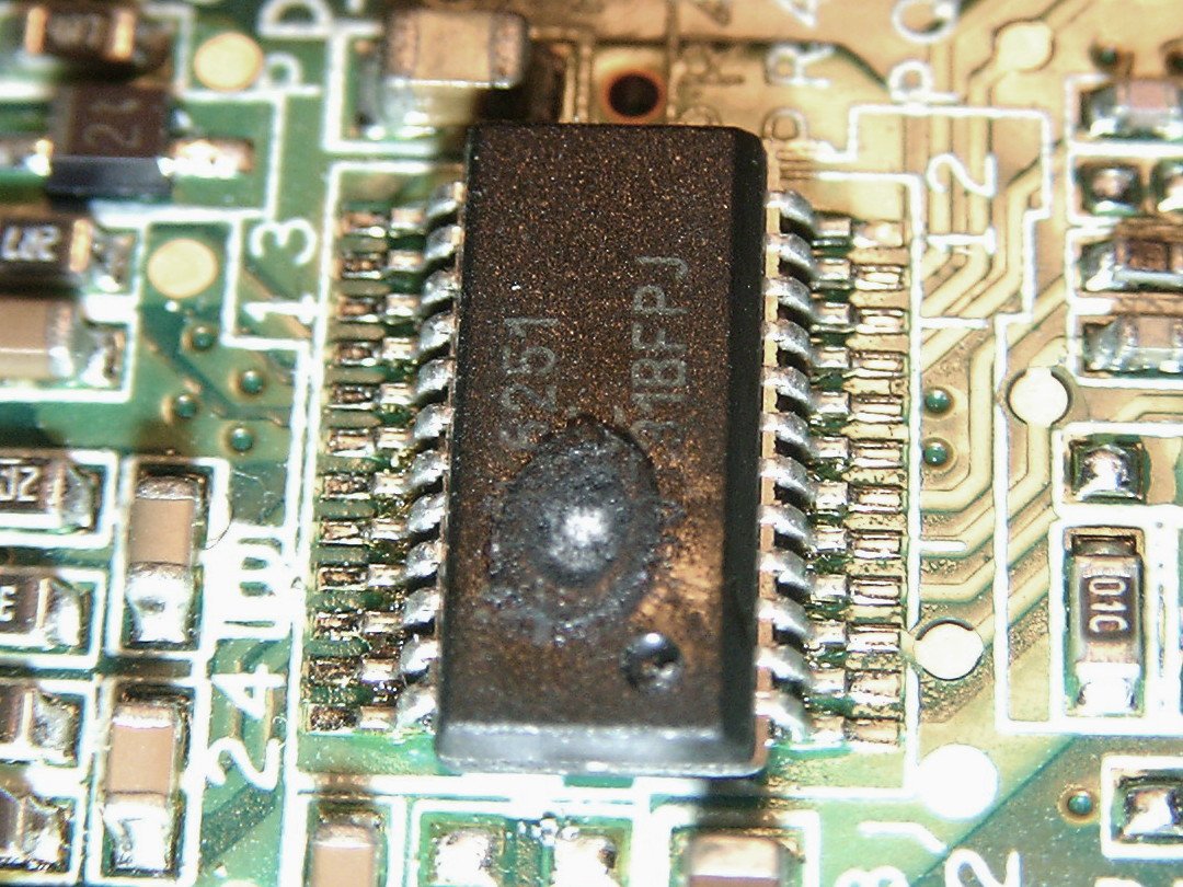
PFA applications span a wide range of devices, including OLED and AMOLED displays, microLEDs, flip-chip packages, high-bandwidth memory, through-silicon vias, and MEMS. Common defects—cracks, voids, delamination, poor contacts—often require deep cross sections for analysis. Mechanical sawing or polishing can induce stress or damage, while plasma FIB avoids mechanical stress but struggles with throughput. Integrating lasers into large-volume workflows addresses these limitations.
Demonstrations by 3D-Micromac AG and TESCAN have shown the effectiveness of this approach. In one case, a 12-mm memory chip was sectioned with a 1-mm-deep cut to expose stacked dies, followed by plasma FIB polishing for SEM inspection. Another example involved preparing a 2-mm-wide trench in a flip-chip package, with the laser dramatically reducing preparation time before FIB refinement.
Correlative workflows further enhance efficiency. By combining laser ablation with computed tomography and FIB systems, engineers can navigate samples using circuit layouts or image overlays, bookmarking regions of interest for precise cross-sectioning. This method is particularly valuable for AMOLED displays, where thin-film transistor layers lie hundreds of microns beneath thick glass substrates and organic layers. Mechanical cutting risks delamination, but with optimized laser parameters, mechanical stress is negligible and debris minimal.
Time savings from laser-assisted preparation can reach 60% to 70% compared to conventional FIB-only methods. Newer laser sources promise even greater reductions, making previously uneconomical analyses feasible. As ultrashort-pulsed lasers continue to integrate into semiconductor diagnostics, they enable faster, cost-effective, and precise workflows that keep pace with the increasing complexity of modern microelectronics.